The world of printed circuit board (PCB) design is changing fast and artificial intelligence (AI) is one of the major players in that transformation. With the arrival of AI-powered design tools, many are wondering if these technologies will eventually make the traditional role of PCB engineers obsolete. Let’s break down how AI is impacting PCB design and manufacturing, what it means for professionals in the field and why the collaboration between human expertise and AI is the key to future success.
Revamping PCB Design: A New Era Begins
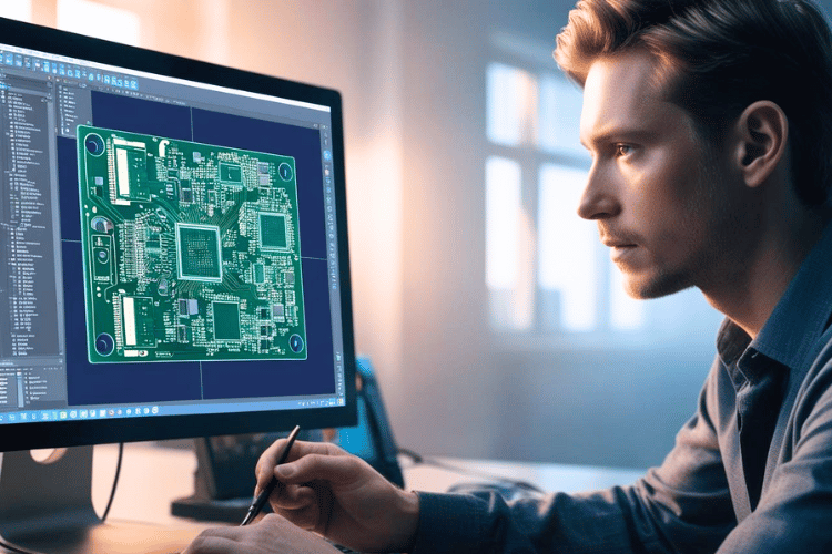
For years, PCB design was an hour of detailed manual work. Engineers accurately drafted board layouts, routed connections one by one and repeatedly checked every detail to ensure everything worked perfectly. This process is rewarding in its own right but it is also slow, labor-intensive and prone to human error.
Today, however, the industry is witnessing a transformation. AI has emerged as an innovative force in PCB design, revolutionizing traditional methods. Modern AI-powered tools now analyze intricate designs, suggest improvements and even predict potential issues before they become major problems. This shift is not just about speeding up the process, it’s about increasing reliability and allowing engineers to focus on innovation rather than routine tasks.
Welcome, AI: Your New Design Partner
Imagine working on a complex PCB layout and having a tool that quickly examines through vast amounts of data to identify the best routing paths, optimal component placements and potential thermal issues. AI does exactly that. It acts like a highly efficient design assistant that processes information in seconds - a task that might have taken hours or even days manually.
These smart tools use machine learning algorithms to learn from previous designs and industry best practices. They offer real-time suggestions, ensuring that every design iteration moves closer to perfection. By handling repetitive and time-consuming tasks, AI frees engineers to tackle more challenging aspects of design such as creative problem-solving and strategic planning. The result is a smoother, faster and more efficient workflow that doesn’t compromise on quality.
Ways How Artificial Intelligence is Improving PCB Design?
Artificial intelligence is revolutionizing PCB design, delivering significant improvements in efficiency, quality and reliability. In today’s fast-paced competitive environment, AI has emerged as an indispensable assistant for designers and manufacturers. Here are several key ways AI is driving change in the PCB industry.

- Improved Component Verification and Defect Detection - Low quality components and subtle defects can compromise PCB reliability. Advanced computer vision systems and deep learning algorithms are used to detect out-of-spec parts and surface issues like spurs, mouse bites, short circuits and open circuits. Enhanced inspection processes ensure that only quality components progress, reducing waste and accelerating product validation.
- Routing Optimization - AI-powered design tools streamline the routing process by quickly analyzing design data. Machine learning algorithms trained on historical data predicts routing congestion, suggest optimal trace paths and identify potential crosstalk issues. This capability not only cuts down design time and costs but also minimizes errors early in the process, leading to more reliable designs.
- Enhancing Signal Integrity - Ensuring high signal integrity is critical for modern PCB assemblies. AI models employ neural networks, genetic algorithms and other techniques to fine-tune interconnect parameters. These predictive models help maintain performance standards while avoiding the need for multiple design iterations. Early adjustments based on AI recommendations result in improved signal quality and a more robust final product.
- Optimized Reflow Soldering and Design Assistance - AI also plays a vital role in the reflow soldering process by predicting ideal temperature profiles and conveyor speeds for complex assemblies. Moreover, AI design assistants learn from past projects, providing valuable suggestions to improve performance, testability and production success. While these tools significantly boost efficiency, human expertise remains crucial to verify complex designs and address errors.
In essence, the collaboration between AI and experienced engineers is paving the way for smarter, more reliable PCB design in a dynamic, competitive market.
Human Creativity Remains King
Despite the impressive capabilities of AI, it’s important to remember that PCB design is as much an art as it is a science. At its core, designing a PCB involves understanding complex electronic systems, anticipating the needs of end users and making decisions that balance performance, cost and reliability. These are tasks that require creative problem-solving, an area where human expertise still excels.
AI may be able to crunch numbers and generate suggestions based on data patterns but it cannot replace the intuitive judgment that comes from years of experience. Human engineers bring context to the table, they understand the delicate points of a project that no algorithm can fully capture. In many cases, the best outcomes are achieved when human insight is combined with AI’s analytical prowess.
Upgrading Skills: Embracing the AI-Driven Future
The rise of AI in PCB design is not a signal that traditional skills are becoming obsolete. Instead, it highlights the importance of evolving and expanding one’s expertise. Today’s engineers are encouraged to develop skills that blend traditional design principles with modern AI tools. Continuous learning has become an essential part of staying competitive in the industry.
Training programs, online courses and hands-on workshops are more popular than ever as professionals seek to understand the latest AI technologies and their practical applications in PCB design. This shift is creating a more versatile workforce that is better prepared to handle the complex challenges of modern electronics. Embracing AI is less about replacing existing skills and more about enhancing them to drive innovation.
Debunking the Myth: Will Engineers Be Replaced?
A common question in the wake of AI advancements is whether human engineers will eventually be replaced. The short answer is no. While AI can take over many of the repetitive and routine aspects of PCB design, the creative and strategic process of the job still require a human touch.
AI excels at processing vast amounts of data and identifying patterns but it lacks the ability to fully understand context, appreciate design delicacies or innovate in ways that break traditional boundaries. The role of the engineer is evolving from being solely a creator to becoming a manager of sophisticated tools that enhance creativity and efficiency.
Rather than fearing replacement, the industry is witnessing a redefinition of roles. Engineers now have the opportunity to focus on higher-level tasks that add value to the design process. This includes strategic decision-making, system-level thinking and creative problem-solving are the areas where human intelligence remains indispensable.
Tackling the Challenges
Of course, the integration of AI into PCB design is not without its challenges. One major concern is the potential for over-reliance on automated systems. If engineers start to depend too heavily on AI, there’s a risk that the human skill set could wasting away over time. To counteract this, it’s important for professionals to maintain a balance by leveraging AI for its strengths while continually improving their own expertise.
Another challenge lies in the need for strong data security and ethical practices. As AI systems become more integrated into design workflows, ensuring that these tools are secure and that the data they process is handled responsibly becomes paramount. The industry must adopt strict standards to safeguard intellectual property and maintain trust in these emerging technologies.
The Road Ahead: A Balanced Outlook
The integration of AI into PCB design is not an indication of job loss, it’s a signal of change and progress. While AI brings incredible speed and efficiency to the table, the human touch remains essential for creativity, problem-solving and strategic decision-making. The future of PCB design is set to be a balanced blend of machine precision and human insight.
As the industry moves forward, the best outcomes will emerge from collaboration. Engineers will continue to play a critical role using AI as a tool to push the boundaries of what’s possible. In this new landscape, the focus shifts from a fear of replacement to an embrace of opportunity - a chance to elevate the practice of PCB design to new heights.
The debate over whether AI will replace PCB engineers misses the bigger picture. Instead of viewing AI as a competitor, it should be seen as a powerful assistant. One that enhances productivity, improves quality and frees up human talent to focus on what matters most i.e., innovation. The evolution of PCB design is not about choosing between humans and machines, but about finding the perfect blend of both.
In an industry where precision and creativity go hand in hand, the future looks bright. As AI continues to evolve, it will undoubtedly open up new avenues for growth and development. Rather than replacing engineers, AI is set to redefine their role-transforming everyday challenges into opportunities for breakthrough innovation.
AI-Enabled PCB Design Tools
Here are several PCB design tools integrating AI capabilities that support automated schematic suggestions, intelligent routing and collaborative workflows for efficient and precise execution of printed circuit board development.
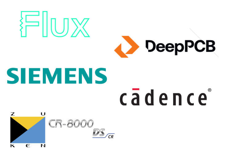
1. Cadence Allegro X Design Platform
The Cadence Allegro X Design Platform is an AI-powered PCB design solution offering advanced automation, multi-domain collaboration and in-design analysis. It enhances design efficiency with AI-driven layout optimization and seamless integration across schematic capture, PCB layout and system analysis.
Key Features:
- AI-powered Generative PCB Layout for optimized component placement
- In-design analysis for real-time simulation and verification
- Constraint-driven design with automated rule checking
- ECAD-MCAD co-design for smooth collaboration between electrical and mechanical engineers
- SPICE simulation with PSpice for analog and mixed-signal analysis
- Rigid-Flex design with 3D visualization and stack-up management
- Concurrent PCB Team Design enabling real-time global collaboration
- Design for Manufacturing (DFM) checks to reduce errors and ensure manufacturability
- PLM Integration with leading product lifecycle management systems
- Multi-domain system design supporting electrical, mechanical and thermal workflows
2. Zuken CR-8000 Series
The Zuken CR-8000 Series is an advanced AI-driven PCB design software offering a fully integrated, end-to-end solution from system architecture to manufacturing optimization. It supports multi-board PCB design, signal integrity analysis, chip/package/board co-design and MCAD integration for complex electronic systems.
Key Features:
- Supports multi-board partitioning, system verification and wire harness integration.
- Provides integrated simulation and analysis for signal integrity (SI), power integrity (PI) and thermal characteristics.
- Incorporates AI-based design optimization for improved performance and layout efficiency.
- Supports single and multi-die packages including flip-chip and advanced packaging.
- Pre-layout and post-layout SI/PI/EMI analysis with third-party integrations (Ansys, Keysight).
- Enables 3D PCB modeling and mechanical integration for multi-board systems.
- Engineering Data Management (PLM Integration), DS-CR for WIP design data management, design re-use and supply chain synchronization.
- Embedded manufacturing verification to ensure high-quality PCB fabrication.
- IPC-2581-based wire harness design synchronization with PCB layouts.
3. DeepPCB
DeepPCB is an AI-powered, fully autonomous PCB design tool leveraging reinforcement learning for PCB routing and component placement. It iteratively refines layouts to deliver DRC-clean designs with minimized vias and optimized signal integrity. DeepPCB integrates seamlessly with existing design workflows, allowing users to start routing from scratch or enhance existing designs, thereby accelerating the design process.
Key Technical Features:
- Reinforcement Learning-based routing and placement automation
- Iterative layout refinement ensuring DRC compliance
- Integration with standard file formats and existing design tools
- Optimization for minimized vias and enhanced signal integrity
4. Siemens Xpedition Enterprise
Siemens Xpedition Enterprise is a next-generation PCB design platform that streamlines the process from concept to manufacture. It offers an intuitive modern UI, AI-infused design support and cloud-connected collaboration. Integrated digital threads enable real-time verification and managed access ensures secure IP protection, optimizing resource management and accelerating time-to-market.
Key Technical Features:
- Intuitive modern UI
- AI-infused design support
- Cloud-connected collaboration
- Integrated digital threads
- Managed access for secure IP protection
5. Flux PCB Design Platform
Flux is a web-based PCB design platform that integrates AI-driven tools to streamline PCB design automation. It supports real-time collaboration, data-driven design workflows and continuous iteration. The system is accessible directly from the browser, eliminating installation requirements while offering design assistance through its integrated Copilot and support versatile functionality.
Key Features:
- Operates entirely within a web browser, requiring no software downloads or installations
- Uses AI to recommend and create schematic connections
- Provides a one-click solution for routing designs with intuitive, human-like result
- Enables multiple users to work together simultaneously with clear permission controls