Ever thought of designing your own IC for a specific boolean logic application? Say you want to design an IC where it dispenses Tea, Coffee, Milk-based on the input choice given in an automated cafeteria or you want to actuate mechanical components/light/tasks depending upon the conditions. Boolean logic plays a major role in our day-to-day life. Well, boolean logic is predominantly used in assembly and computer programming languages, building digital logic circuits, computer architectures, machine languages, decision making both in software and hardware for conditional scenarios, and so on applications in modern technologies. Being an electronic enthusiastic, one needs to understand how to implement Boolean expression in VHDL.
Now, let us take a simple Boolean Expression/logic that your application-specific IC has to implement as given below.

In this article, we will learn how to implement the Boolean Expression/Logic in VHDL using Data Flow, Behavioral, structural modelling. All these three types of modellings are pretty much the same, but there are some modifications that have to be done in the architecture declaration part of the VHDL program. Also, we have to write a Testbench to verify the authenticity of the circuit built using the VHDL.
To know about the general structure of a VHDL code, what are the three types of VHDL Modelling and its significance, why VHDL modelling is used, and what is Test Bench; refer to - Getting Started with VLSI and VHDL using ModelSim.
So, now that we know the basics of VHDL Coding and VHDL Modelling, let’s calculate the Truth Table values for the above equation.
The values for the Y with the inputs P, Q, R are tabulated below.
|
P |
Q |
R |
|
|
0 |
0 |
0 |
0 |
|
0 |
0 |
1 |
0 |
|
0 |
1 |
0 |
1 |
|
0 |
1 |
1 |
1 |
|
1 |
0 |
0 |
0 |
|
1 |
0 |
1 |
1 |
|
1 |
1 |
0 |
1 |
|
1 |
1 |
1 |
1 |
Data Flow Modelling
As discussed earlier during our previous tutorial “Getting Started with VLSI and VHDL using ModelSim—A beginner's Guide”, in this type of modelling the output is mapped to the Boolean Equation with the variables P, Q, R. So, first let us know how to write the code fully and then break down them into separate segments. Just use the complete code given below for Data Flow Modelling.
Full Code for Data Flow Modelling
Library IEEE;
use ieee.std_logic_1164.all;
entity bool_exp_data is
    port(inp : in std_logic_vector(2 downto 0);
         Y : out std_logic);
end bool_exp_data;
architecture data of bool_exp_data is
 begin
Y<= (inp(2) and inp(1)) or (inp(2) and inp(1) and inp(0)) or ( not(inp(2)) and inp(1) )  or  (  inp(2) and   not ( inp(1)) and inp(0)    )
end data;
Let's break the entire code and analyze how data flow modelling is performed.
The first step is to import the IEEE Library.
Library IEEE;
use ieee.std_logic_1164.all;
The second step is to declare the entity. There are some changes in the entity declaration when compared to the previous tutorial “Implementation of Basic Logic Gates”. Let's see the changes in the entity declaration segment.
The entity is declared with the name “bool_exp_data” and the input and the output are declared. Since the input involves three variables, it would be a time-consuming process to simulate the output by assigning the inputs each time for the three variables.
So, let's make our code a little smarter!
Instead of using “std_logic” which is a standard signal, the inputs are given as an array/vectors of the signal by using std_logic_vector.
“std_logic_vector” is a method of declaring a signal as an array.
The input signal is declared as “inp”. Here, std_logic_vector is used for declaring the signal as an input of arrays/vectors. The std_logic_vector of the signal “inp” indexing starts from 2 and ends at 0 as we have 3 variables P, Q, R. The indexing of the input signal is shown below. The phrase “2 down to 0” indicates that it descends from 2 to 0. The input signal “inp” has three values namely inp(2), inp(1), inp(0). Since the output(Y) is either 0/1 a standard signal is sufficient, so the output Y is declared using “std_logic”.
|
Indexing_number |
2 |
1 |
0 |
|
inp signal |
inp(2) |
inp(1) |
inp(0) |
For example, if the signal “inp” has the value “101” then inp(2)=>1, inp(1)=>0, inp(0)=>1.
Now, we have three variables P, Q, R so these variables are mapped to the signal “inp”
inp(2)=> P, inp(1)=> Q, inp(0)=> R. So these variables are mapped to the input signal.
|
Variable |
P |
Q |
R |
|
inp signal |
inp(2) |
inp(1) |
inp(0) |
The below-given snippet is the entity declaration segment.
entity bool_exp_data is
    port(inp : in std_logic_vector(2 downto 0);
         Y : out std_logic);
end bool_exp_data;
After the entity is declared, the architecture for the entity should be declared where data flow modelling is implemented. Let's dig deep into the code on data flow modelling.
The output Y is mapped to the Boolean expression. For example, in the equation , P and Q are subjected to “AND” operation, the signal values inp(2) and inp(1) are subjected to AND operation(inp(2) and inp(1)). Next AND operation of PQR, so “inp(2) and inp(1) and inp(0)” is declared.
Similar to the Boolean expression, the output Y signal is mapped to the Boolean operations between the variables inp(2), inp(1), inp(0). In simpler terms, the Boolean expression is written in terms of the Boolean operators “AND, OR, NOT” and performed among the values of the “inp” signal.
architecture data of bool_exp_data is
 begin
Y<= (inp(2) and inp(1)) or (inp(2) and inp(1) and inp(0)) or ( not(inp(2)) and inp(1) )  or  (  inp(2) and   not ( inp(1)) and inp(0)    );
end data;
Just copy-paste the Full Code for Data Flow Modelling in the Modelsim and compile it. The procedures for compiling and simulating the waveform are given in the previous tutorial “Implementation of Basic Logic Gates using VHDL in Modelsim”.
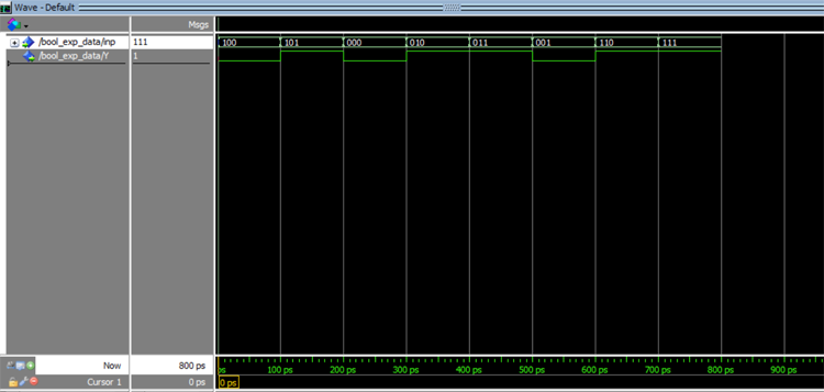
I have compiled and simulated the code and generated the waveforms, and the input, outputs are generated as given in the waveform figure.
So, now from the above waveform, we can see that the inputs are in the form of vectors and the outputs are 0/1 waveform. The corresponding outputs for the input vectors from the graph are tabulated below. Move the cursor along 0-800 ps to notice the change in corresponding inputs and outputs. Verify these waveform values with the Truth Table and you can infer that the values are corresponding.
|
Timing (ps) |
inp (inp(2)=>P, inp(1)=>Q, inp(0)=>R ) |
Y |
|
0-100 |
100 |
0 |
|
100-200 |
101 |
1 |
|
200-300 |
000 |
0 |
|
300-400 |
010 |
1 |
|
400-500 |
011 |
1 |
|
500-600 |
001 |
0 |
|
600-700 |
110 |
1 |
|
700-800 |
111 |
1 |
So, this is how data flow modelling of circuits is designed in VHDL.
Behavioral Modelling: Only change in the Behavioral modelling is in the architecture declaration segment of the code. The library declaration and the entity remain the same. So, let's get to know what changes have to be done for behavioral modelling.
In this modelling, the circuits are designed using certain conditions/scenarios. The circuits are instructed to switch outputs based upon the specified conditions. As the name itself suggests, behavioral modelling describes how the circuit should behave.
Here, we have two scenarios from the Truth Table for the Boolean Expression, Output being 1 or 0 for the possible 8 inputs. The scenarios are given below.
|
Scenario |
inp (inp(2)=>P, inp(1)=>Q, inp(0)=>R ) |
Output (Y) |
|
1 |
000,001,100 |
0 |
|
2 |
010,011,101,110,111 |
1 |
So, for inputs 000,001,100, the output (Y) is 0 and for the remaining inputs, the output (Y) is 1.
The Code for Behavioral Modelling is given below.
Library IEEE;
use ieee.std_logic_1164.all;
entity bool_exp_behav is
    port(inp : in std_logic_vector(2 downto 0);
         Y : out std_logic);
end bool_exp_behav;
architecture sim of bool_exp_behav is
 begin
 process(inp)
begin
if(inp="000" or inp="001" or inp="100") then
Y<='0';
else
Y<='1';
end if;
end process;
end sim;
The library is declared, and The entity is defined as “bool_exp_behav” with “inp” as input and “Y” as output.
Note: The entity name can be of your choice, any name is expected. But make sure that the same name is used in architecture defining.
Now, let's see how to define the architecture for behavioral modelling. If-else statements are used for behavioral modelling.
architecture sim of bool_exp_behav is: The architecture is given by the name/defined with the name “sim”.
Note: The architecture name can be any name of your choice. Here the architecture name is “sim”.
process(inp): Since the Output is dependent on the input signal “inp” and the decisions are taken depending upon the “inp”, the signal “inp” should be processed. So “process(inp)” is initiated first.
Begin: If a process is initiated, then the process should begin. So, it is mandatory that if a process is defined it should be followed by begin.
After that the processes have begun, we should specify the conditions. So, simple if-else statements are used for the scenarios. Refer to the scenario table above. So, for the inputs are 000,001,100, then Y equals 1 else Y equals 0.
Once the if-else statements are declared, the if process should be terminated, so we use “end if;” and once the process is finished, the process should be terminated hence “end process:” is used to terminate the process and finally the architecture declaration should be terminated, hence “end sim;” is used.
architecture sim of bool_exp_behav is
 begin
 process(inp)
begin
if(inp="000" or inp="001" or inp="100") then
Y<='0';
else
Y<='1';
end if;
end process;
end sim;
The above code is compiled, simulated and the results can be verified from the waveform figure below.
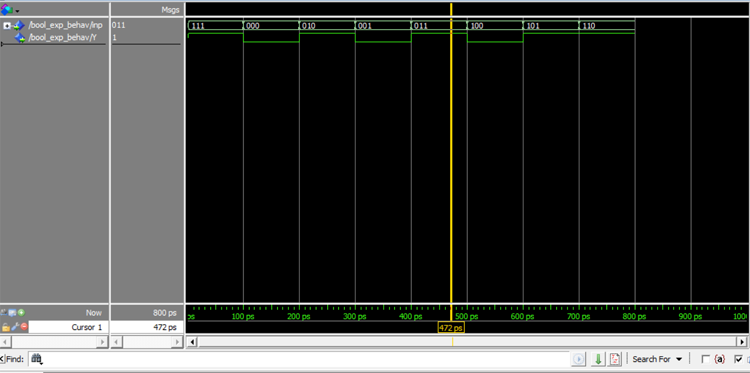
So, first I give the input as 111, the output is 1, then next input is given as 000 the output is 0. Try giving all other possible combinations of inputs. Move the yellow cursor from 0-800 ps to find the corresponding inputs and outputs.
|
Timing(ps) |
inp |
Y |
|
0-100 |
111 |
1 |
|
100-200 |
000 |
0 |
|
200-300 |
010 |
1 |
|
300-400 |
001 |
0 |
|
400-500 |
011 |
1 |
|
500-600 |
100 |
0 |
|
600-700 |
101 |
1 |
|
700-800 |
110 |
1 |
The waveform from 0-800ps is given above, which equals the Truth Table.
Structure Modelling:
Structure Modelling involves the interconnection of sub-components. To get an outlook of structural modelling refer to “Getting Started with VLSI and VHDL using ModelSim—A beginner's Guide”
From the equation , we can infer that the required gates are OR, AND, NOT gates. So these components are interconnected to form the circuit.
The circuit for the Boolean expression is given below.

Now, let's see the structure modelling code and what all has to be declared in the architecture.
Structure Modelling Code:
Library IEEE;
use ieee.std_logic_1164.all;
entity bool_structure is
    port(inp : in std_logic_vector(2 downto 0);
         final : out std_logic);
end bool_structure;
architecture sim of bool_structure is
 component anddd_gaate is
    port(A : in std_logic;
         B : in std_logic;
         Y : out std_logic);
end component;
component or_gate is
    port(A : in std_logic;
         B : in std_logic;
         Y : out std_logic);
end component;
component not_gate is
    port(A : in std_logic;
         Y : out std_logic);
end component;
signal T1,T2,T3,T4,T5,T6,T7,T8,T9,T10:std_logic ;
begin
---PQ----
k: anddd_gaate port map(A=>inp(2), B=>inp(1), Y=>T1);
---PQR----
and2:anddd_gaate port map(A=>inp(0),B=>T1,Y=>T2);
--OR PQ+PQR----
or1:or_gate port map(A=>T1,B=>T2,Y=>T3);
-----notp-----
not1: not_gate port map(A=>inp(2),Y=>T4);
-----NOTP.Q--------
and3:anddd_gaate port map(A=>T4,B=>inp(1),Y=>T5);
---------PQ+PQR+NOTPQ----
or2:or_gate port map(A=>T3,B=>T5,Y=>T6);
---notq----
not2: not_gate port map(A=>inp(1),Y=>T7);
-----notq and P------
and4:anddd_gaate port map(A=>T7,B=>inp(2),Y=>T8);
----pqr--------
and5:anddd_gaate port map(A=>T8,B=>inp(0),Y=>T9);
or3:or_gate port map(A=>T6,B=>T9,Y=>T10);
final<=T10;
end sim;
The entity is declared with entity name as “bool_strcuture” with “inp” as input signal and “final” as an output signal.
Here comes the important segment, the architecture declaration segment of the code. I have given the architecture declaration snippet below.
architecture sim of bool_structure is: The architecture is defined with the name “sim”.
As said earlier, Behavioral modelling is about interconnecting the components, we should define the sub components in the architecture. This is similar to a function that is used in a programming language where a function is defined and is called back in the latter. So before starting the behavioral modelling, it is mandatory to script and successfully compile the “OR, AND, NOT” gates.
Refer to the previous article “Implementation of Basic Logic Gates using VHDL in Modelsim” for the implementation of basic logic gates. These basic gate codes are used for structural modelling. So, the sub-components are declared with the phrase “component” instead of an entity. Just copy past the entity declaration of the basic logic gates and replace the phrase “entity” with the phrase “component”. Earlier when the “OR, AND, NOT” gates were designed by the entity names “anddd_gate,or_gate,not_gate” respectively. The same names should be used while declaring the component.
architecture sim of bool_structure is
 component anddd_gaate is
    port(A : in std_logic;
         B : in std_logic;
         Y : out std_logic);
end component;
component or_gate is
    port(A : in std_logic;
         B : in std_logic;
         Y : out std_logic);
end component;
component not_gate is
    port(A : in std_logic;
         Y : out std_logic);
end component;
signal T1,T2,T3,T4,T5,T6,T7,T8,T9,T10:std_logic: These signals are the intermediate outputs of the gate which act as the input to the next gate. The corresponding outputs are tabulated below and refer to the circuit diagram above. To declare a signal, the syntax is just “signal singnal_name: std_logic”.

signal T1,T2,T3,T4,T5,T6,T7,T8,T9,T10:std_logic;
Now that we have assigned the signals, we have to map the corresponding signals with appropriate blocks. This is called port mapping where the wires are interconnected.
The syntax is Component label : component name port map(input=>output);
The component label can be any name, it is just a name, but make sure that the labels are not repeated. The component name should be the same as the component declared previously. Port Map connects the corresponding inputs and outputs accordingly.
For example, for the expression “PQ” in the Boolean expression, we need AND gate.
So P is inp(2) and Q is inp(1), AND operations should be performed. So these two values act as the input to the NAD gate so “port map (A=>inp(2), B=>inp(1), Y=>T1)” where A and B is the input of the AND gate and Y is the output of AND gate.
So what happens is “A=>inp(2)” A takes the value of inp(2) and “B=>inp(1)” B takes the value of inp(1) and Y is mapped to the intermediary signal T1. So the value of the signal T1 will be AND operation of inp(2) and inp(1).
Similarly, each component is declared accordingly and their inputs and output signals are mapped. Refer to the comments in the code and the circuit diagram. T10 is the final output, so the signal “final” which is declared as the output is mapped to T10. So the “final” signal takes the value of T10.
The code for interconnecting the sub-components is given below.
begin
---PQ----
k: anddd_gaate port map(A=>inp(2), B=>inp(1), Y=>T1);
---PQR----
and2:anddd_gaate port map(A=>inp(0),B=>T1,Y=>T2);
--OR PQ+PQR----
or1:or_gate port map(A=>T1,B=>T2,Y=>T3);
-----notp-----
not1: not_gate port map(A=>inp(2),Y=>T4);
-----NOTP.Q--------
and3:anddd_gaate port map(A=>T4,B=>inp(1),Y=>T5);
---------PQ+PQR+NOTPQ----
or2:or_gate port map(A=>T3,B=>T5,Y=>T6);
---notq----
not2: not_gate port map(A=>inp(1),Y=>T7);
-----notq and P------
and4:anddd_gaate port map(A=>T7,B=>inp(2),Y=>T8);
----p notq r--------
and5:anddd_gaate port map(A=>T8,B=>inp(0),Y=>T9);
or3:or_gate port map(A=>T6,B=>T9,Y=>T10);
final<=T10;
Copy-paste the entire code for Structure Modelling, compile and simulate the waveforms with different input vectors. The sample waveform graph is given below.
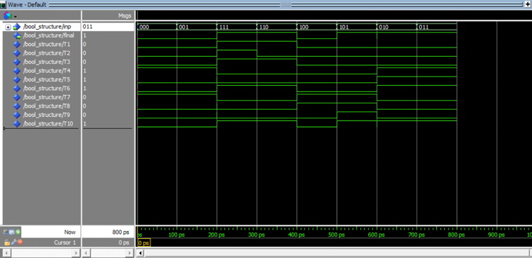
The value of the signal from the waveform is shown below.
|
Timing(ps) |
inp |
final |
|
0-100 |
000 |
0 |
|
100-200 |
001 |
0 |
|
200-300 |
111 |
1 |
|
300-400 |
110 |
1 |
|
400-500 |
100 |
0 |
|
500-600 |
101 |
1 |
|
600-700 |
010 |
1 |
|
700-800 |
011 |
1 |
We are at the end of this tutorial. Now we know how to design using all three models. The next crucial step is to test the circuit.
Test Bench Code for Boolean Expression
Test Bench is used to test whether the designed circuit/system is functioning properly with the input test vectors given. So, the system/circuit is subjected to testing. The system under the test is generally called a Device under test (DUT).
So rather than giving inputs each time and simulating each time, in the test bench, a set of input vectors are given at a time and tested so that it reduces the time involved in testing. When dealing with complex circuits, Test Bench will make the tasks easier for the verification of the design.
We can take any type of modelling that we want to test. In this example, I am choosing the dataflow model. So now the data flow model is the DUT.
Test Bench code:
LIBRARY ieee;
USE ieee.std_logic_1164.ALL;
ENTITY testbench_bool IS
END testbench_bool;
ARCHITECTURE sim OF testbench_bool IS
 component bool_exp_data is
    port(inp : in std_logic_vector(2 downto 0);
         Y : out std_logic);
end component;
 ----Inputs
 signal test_input : std_logic_vector (2 downto 0) := "000";
--OUTPUTS--
 signal test_output : std_logic;
BEGIN
 dut: bool_exp_data PORT MAP (inp => test_input,Y=>test_output);
 process
 begin
 wait for 0.1 ns;
test_input<="101";
 wait for 0.1 ns;
test_input<="001";
wait for 0.1 ns;
test_input<="010";
wait for 0.1 ns;
test_input<="011";
wait for 0.1 ns;
test_input<="100";
wait for 0.1 ns;
test_input<="110";
wait for 0.1 ns;
test_input<="111";
wait for 0.1 ns;
test_input<="000";
wait for 0.1 ns;
end process;
END;
There are little modifications that have to be done both in entity declaration and architecture declaration.
I will break down the code and explain what changes have to be done for Test Bench.
The libraries are imported, and the entity is declared with the name “testbench_tool”. Here, we may notice that inputs and outputs aren’t declared. This is because the input and the outputs are already declared for the data flow modelling. Instead, we just need to connect a signal in which the input vectors will pass through.
LIBRARY ieee;
USE ieee.std_logic_1164.ALL;
ENTITY testbench_bool IS
END testbench_bool;
Now the architecture is defined, and the data flow modelling function is called under the architecture. This is similar to the structure modelling where the previously defined functions are used.
ARCHITECTURE sim OF testbench_bool IS
 component bool_exp_data is
    port(inp : in std_logic_vector(2 downto 0);
         Y: out std_logic);
end component;
Since we didn’t declare the input in the entity declaration, we assign “test_input” as the input signal.
The signal “test_input” is initialized with the value “000”.
The signal “test_output” is defined as the output signal
----Inputs
 signal test_input : std_logic_vector (2 downto 0) := "000";
--OUTPUTS--
 signal test_output : std_logic;
Once the signals are declared, port mapping is done, so the “inp” signal will take the values of the test_input and “Y” is mapped to test_output. The values of test_output take the value of Y.
dut: bool_exp_data PORT MAP (inp => test_input,Y=>test_output);
Now all signals and components being declared let us automatically force values to the signals.
wait for 0.1 ns;Initially there is a delay for 0.1 ns.
1 ns = 1000 ps. Which mean there is delay for 100 ps.
Now the 8 possible vector values are passed to the signal “test_input”. There is a delay of 100 ps for each vector which means each value will be present up to 100ps.
wait for 0.1 ns;
test_input<="101";
 wait for 0.1 ns;
test_input<="001";
wait for 0.1 ns;
test_input<="010";
wait for 0.1 ns;
test_input<="011";
wait for 0.1 ns;
test_input<="100";
wait for 0.1 ns;
test_input<="110";
wait for 0.1 ns;
test_input<="111";
wait for 0.1 ns;
test_input<="000";
wait for 0.1 ns;
end process;
So there is a total 0.9 ns delay in the entire record. So while running the code run it for 900 ps in the run-length box.

The same is simulated, and the values are verified against the Truth Table. So with this test bench, we can make the testing process efficient and quick.
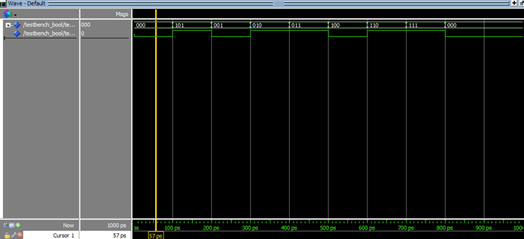
|
Timing(ps) |
test_input |
Test_output |
|
0-100 |
000 |
0 |
|
100-200 |
101 |
1 |
|
200-300 |
001 |
0 |
|
300-400 |
010 |
1 |
|
400-500 |
011 |
1 |
|
500-600 |
100 |
0 |
|
600-700 |
110 |
1 |
|
700-800 |
111 |
1 |
|
800-900 |
000 |
0 |
The above values correspond to the Truth Table of Boolean Expression.
Complete Project Code
Behav.
Library IEEE;

use ieee.std_logic_1164.all;

entity bool_exp_behav is

    port(inp : in std_logic_vector(2 downto 0);

         Y : out std_logic);

end bool_exp_behav;

architecture sim of bool_exp_behav is

 begin

 process(inp)

begin

if(inp="000" or inp="001" or inp="100") then

Y<='0';

else

Y<='1';

end if;

end process;

end sim;

The library is imported

____under BOX--------

Library IEEE;

use ieee.std_logic_1164.all;

---box---

entity bool_exp_behav is

    port(inp : in std_logic_vector(2 downto 0);

         Y : out std_logic);

end bool_exp_behav;
Data
Library IEEE;

use ieee.std_logic_1164.all;

entity bool_exp_data is

    port(inp : in std_logic_vector(2 downto 0);

         Y : out std_logic);

end bool_exp_data;

architecture data of bool_exp_data is

 begin

Y<= (inp(2) and inp(1)) or (inp(2) and inp(1) and inp(0)) or ( not(inp(2)) and inp(1) )  or  (  inp(2) and   not ( inp(1)) and inp(0)    )

end data;

structure

Library IEEE;
use ieee.std_logic_1164.all;
entity bool_structure is
    port(inp : in std_logic_vector(2 downto 0);
         final : out std_logic);
end bool_structure;
architecture sim of bool_structure is
 component anddd_gaate is
    port(A : in std_logic;
         B : in std_logic;
         Y : out std_logic);
end component;
component or_gate is
    port(A : in std_logic;
         B : in std_logic;
         Y : out std_logic);
end component;
component not_gate is
    port(A : in std_logic;
         Y : out std_logic);
end component;
signal T1,T2,T3,T4,T5,T6,T7,T8,T9,T10:std_logic ;
begin
---PQ----
k: anddd_gaate port map(A=>inp(2), B=>inp(1), Y=>T1);
---PQR----
and2:anddd_gaate port map(A=>inp(0),B=>T1,Y=>T2);
--OR PQ+PQR----
or1:or_gate port map(A=>T1,B=>T2,Y=>T3);
-----notp-----
not1: not_gate port map(A=>inp(2),Y=>T4);
-----NOTP.Q--------
and3:anddd_gaate port map(A=>T4,B=>inp(1),Y=>T5);
---------PQ+PQR+NOTPQ----
or2:or_gate port map(A=>T3,B=>T5,Y=>T6);
---notq----
not2: not_gate port map(A=>inp(1),Y=>T7);
-----notq and P------
and4:anddd_gaate port map(A=>T7,B=>inp(2),Y=>T8);
----pqr--------
and5:anddd_gaate port map(A=>T8,B=>inp(0),Y=>T9);
or3:or_gate port map(A=>T6,B=>T9,Y=>T10);
final<=T10;
end sim;

Testbench
LIBRARY ieee;

USE ieee.std_logic_1164.ALL;

ENTITY testbench_bool IS

END testbench_bool;

ARCHITECTURE sim OF testbench_bool IS

 component bool_exp_data is

    port(inp : in std_logic_vector(2 downto 0);

         Y : out std_logic);

end component;

 ----Inputs

 signal test_input : std_logic_vector (2 downto 0) := "000";

--OUTPUTS--

 signal test_output : std_logic;

BEGIN

 dut: bool_exp_data PORT MAP (inp => test_input,Y=>test_output);

 process

 begin

 wait for 0.1 ns;

test_input<="101";

 wait for 0.1 ns;

test_input<="001";

wait for 0.1 ns;

test_input<="010";

wait for 0.1 ns;

test_input<="011";

wait for 0.1 ns;

test_input<="100";

wait for 0.1 ns;

test_input<="110";

wait for 0.1 ns;

test_input<="111";

wait for 0.1 ns;

test_input<="000";

wait for 0.1 ns;

end process;

END;

